- Today
- Holidays
- Birthdays
- Reminders
- Cities
- Atlanta
- Austin
- Baltimore
- Berwyn
- Beverly Hills
- Birmingham
- Boston
- Brooklyn
- Buffalo
- Charlotte
- Chicago
- Cincinnati
- Cleveland
- Columbus
- Dallas
- Denver
- Detroit
- Fort Worth
- Houston
- Indianapolis
- Knoxville
- Las Vegas
- Los Angeles
- Louisville
- Madison
- Memphis
- Miami
- Milwaukee
- Minneapolis
- Nashville
- New Orleans
- New York
- Omaha
- Orlando
- Philadelphia
- Phoenix
- Pittsburgh
- Portland
- Raleigh
- Richmond
- Rutherford
- Sacramento
- Salt Lake City
- San Antonio
- San Diego
- San Francisco
- San Jose
- Seattle
- Tampa
- Tucson
- Washington
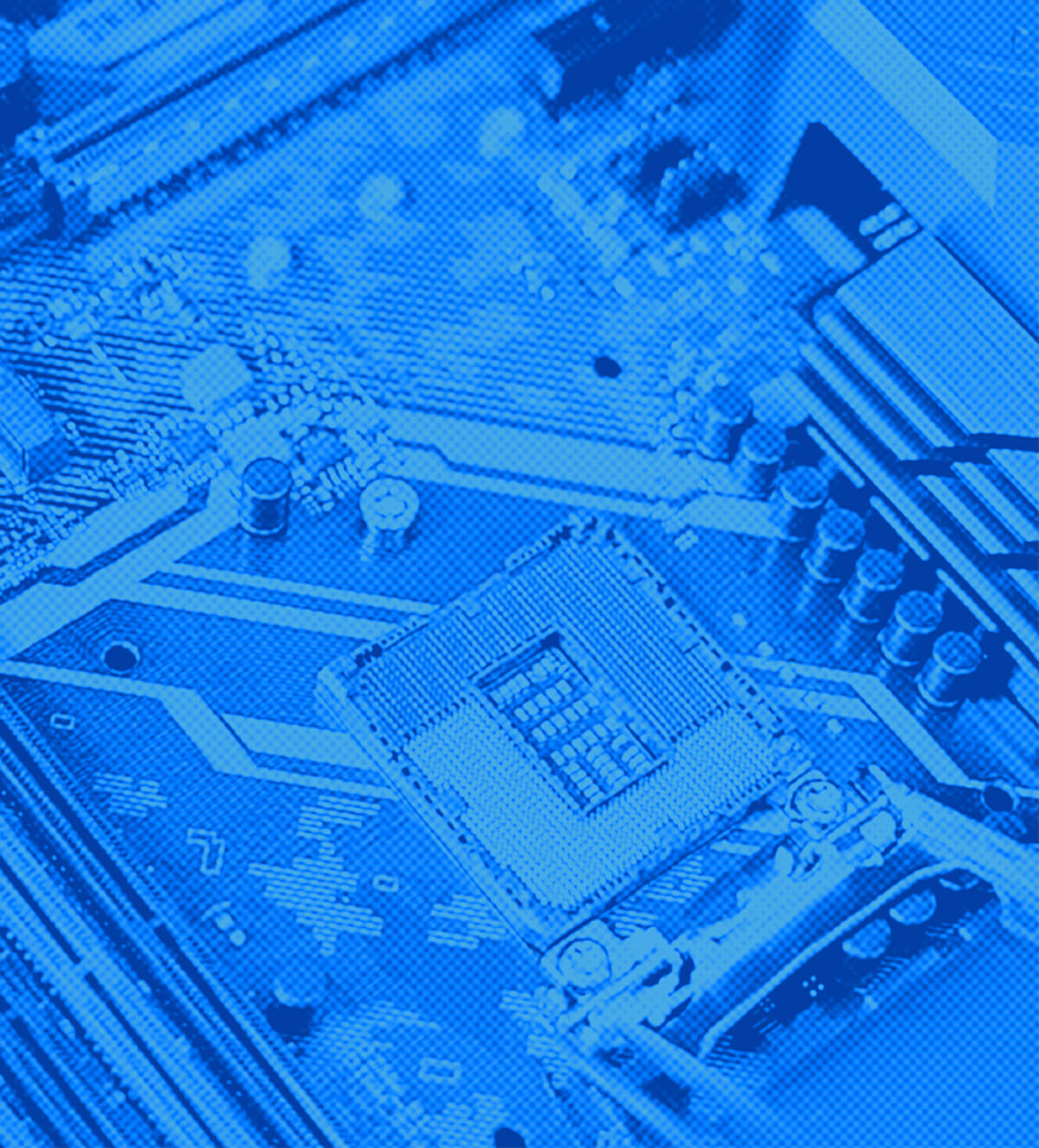
Nearfield Instruments Unveils Sidewall Imaging for 3D Chip Metrology
New mode enables non-destructive, inline 3D sidewall profiling for advanced semiconductor manufacturing.
Published on Mar. 10, 2026
Got story updates? Submit your updates here. ›
Nearfield Instruments has announced the launch of its Sidewall Imaging Mode, a breakthrough measurement capability for its QUADRA high-throughput scanning probe metrology platform. The new mode provides non-destructive, inline 3D sidewall profiling for high-aspect-ratio features in advanced logic and memory devices, enabling chipmakers to monitor next-generation semiconductors with unprecedented precision during process development and high-volume manufacturing.
Why it matters
As the semiconductor industry transitions to fully 3D device architectures driven by the growth of artificial intelligence, detailed sidewall information is crucial for monitoring critical dimensions, variability, and energy efficiency. Sidewall Imaging Mode complements existing techniques like transmission electron microscopy (TEM) by bringing 3D structural analysis inline, enabling faster innovation cycles, higher manufacturing yield, and more energy-efficient AI chips.
The details
Sidewall Imaging Mode extends atomic force microscopy (AFM) using Nearfield's patented cantilever design, sensor fusion, and trajectory control to capture both vertical and lateral interaction forces, enabling full 3D reconstruction of high-aspect-ratio features such as etched gates, nanosheets, and deep memory channels. This non-destructive, inline metrology supports statistical process control and rapid optimization, overcoming the throughput limitations of TEM cross-sectional analysis.
- Nearfield Instruments presented the Sidewall Imaging Mode approach at SPIE Advanced Lithography + Patterning 2026 in San Jose, California.
The players
Nearfield Instruments
An advanced metrology company that has developed the QUADRA high-throughput scanning probe platform with the new Sidewall Imaging Mode capability.
Dr. Hamed Sadeghian
Co-Founder and CEO of Nearfield Instruments, who commented on the importance of 3D metrology for scaling compute performance in next-generation semiconductor technologies.
What they’re saying
“The road to scaling compute performance is vertical, no matter the device. As devices move fully into the third dimension, process control must do the same. Sidewall Imaging Mode enables non-destructive 3D metrology with enough data to support both manufacturing precision and energy-efficient performance. This capability is fundamental for the next generation of AI-driven semiconductor technologies.”
— Dr. Hamed Sadeghian, Co-Founder and CEO (semiconductor-digest.com)
What’s next
Nearfield Instruments is introducing Sidewall Imaging Mode to leading-edge customers and further strengthening its QUADRA platform for advanced 3D logic and memory manufacturing.
The takeaway
Nearfield Instruments' new Sidewall Imaging Mode represents a significant advancement in 3D semiconductor metrology, enabling chipmakers to monitor critical dimensions and process control for the next generation of energy-efficient AI chips with unprecedented precision and throughput.
San Jose top stories


San Jose events

Mar. 11, 2026
San Jose Barracuda vs. San Diego Gulls
Mar. 12, 2026
Phil Hanley
Mar. 13, 2026
Phil Hanley