- Today
- Holidays
- Birthdays
- Reminders
- Cities
- Atlanta
- Austin
- Baltimore
- Berwyn
- Beverly Hills
- Birmingham
- Boston
- Brooklyn
- Buffalo
- Charlotte
- Chicago
- Cincinnati
- Cleveland
- Columbus
- Dallas
- Denver
- Detroit
- Fort Worth
- Houston
- Indianapolis
- Knoxville
- Las Vegas
- Los Angeles
- Louisville
- Madison
- Memphis
- Miami
- Milwaukee
- Minneapolis
- Nashville
- New Orleans
- New York
- Omaha
- Orlando
- Philadelphia
- Phoenix
- Pittsburgh
- Portland
- Raleigh
- Richmond
- Rutherford
- Sacramento
- Salt Lake City
- San Antonio
- San Diego
- San Francisco
- San Jose
- Seattle
- Tampa
- Tucson
- Washington
UCLA Breakthrough Solves Nanoscale Bottleneck in Tech
Researchers develop strategy to improve electrical contact in perovskite semiconductors, a key step toward practical applications.
Mar. 20, 2026 at 7:42am
Got story updates? Submit your updates here. ›
Researchers at UCLA have discovered a way to dramatically improve how electrical current enters perovskite semiconductors, an emerging class of materials with enormous potential for next-generation electronics. The team developed a strategy that creates a very thin, locally modified region under the metal contact, enabling electrons to pass through the barrier using quantum tunneling and reducing resistance at the interface.
Why it matters
Perovskites are a promising class of materials for solar cells, sensors, photodetectors and advanced electronics, but a major obstacle has been poor electrical contact between metal electrodes and the perovskite semiconductor. This research addresses that bottleneck, which could enable faster, lower-power and more reliable perovskite electronic devices, marking an important step toward translating these materials from laboratory research into practical technologies.
The details
The researchers developed a contact-induced charge-transfer doping method using silver oxide nanoclusters formed at the interface. This locally p-doped region beneath the metal contact dramatically narrows the energy barrier, enabling charge carriers to pass through via quantum tunneling rather than traditional thermionic emission. This reduces the resistance at the contact by shrinking the "blocked" region from about 250 nanometers to less than 25 nanometers, allowing current to flow more efficiently at lower voltages.
- The study was published on March 20, 2026.
The players
Xiangfeng Duan
The study's corresponding author, holder of the Raymond A. and Dorothy A. Wilson Endowed Chair and a distinguished professor of chemistry and biochemistry at the UCLA College.
Boxuan Zhou
A UCLA doctoral student and first author on the study.
Laiyuan Wan
A UCLA postdoctoral fellow and first author on the study.
Yu Huang
A CNSI member, holder of the Traugott and Dorothea Frederking Endowed Chair, and a professor of materials science and engineering at the UCLA Samueli School of Engineering.
What they’re saying
“This work addresses a critical bottleneck in perovskite electronics and offers a new design strategy to improve device performance.”
— Xiangfeng Duan, Corresponding author
What’s next
The researchers are currently working to further develop and optimize the contact-induced doping approach, with the goal of enabling faster, lower-power and more reliable perovskite electronic devices.
The takeaway
This breakthrough represents a significant step forward in overcoming a major obstacle to the practical application of perovskite materials in next-generation electronics, paving the way for more efficient, lower-power, and more reliable devices.
Los Angeles top stories


Los Angeles events

Apr. 9, 2026
Testament - Thrash of The Titans
Apr. 9, 2026
KXLU Fundrazor Show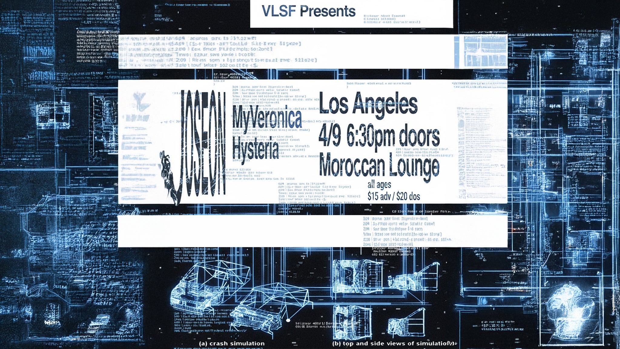
Apr. 9, 2026
VLSF Presents: Joseon with MyVeronica & Hysteria