- Today
- Holidays
- Birthdays
- Reminders
- Cities
- Atlanta
- Austin
- Baltimore
- Berwyn
- Beverly Hills
- Birmingham
- Boston
- Brooklyn
- Buffalo
- Charlotte
- Chicago
- Cincinnati
- Cleveland
- Columbus
- Dallas
- Denver
- Detroit
- Fort Worth
- Houston
- Indianapolis
- Knoxville
- Las Vegas
- Los Angeles
- Louisville
- Madison
- Memphis
- Miami
- Milwaukee
- Minneapolis
- Nashville
- New Orleans
- New York
- Omaha
- Orlando
- Philadelphia
- Phoenix
- Pittsburgh
- Portland
- Raleigh
- Richmond
- Rutherford
- Sacramento
- Salt Lake City
- San Antonio
- San Diego
- San Francisco
- San Jose
- Seattle
- Tampa
- Tucson
- Washington
Perovskite Crystal Lattice Bends, Paving Device Path
New semiconductor materials could enable novel light-responsive devices
Mar. 31, 2026 at 10:38am
Got story updates? Submit your updates here. ›
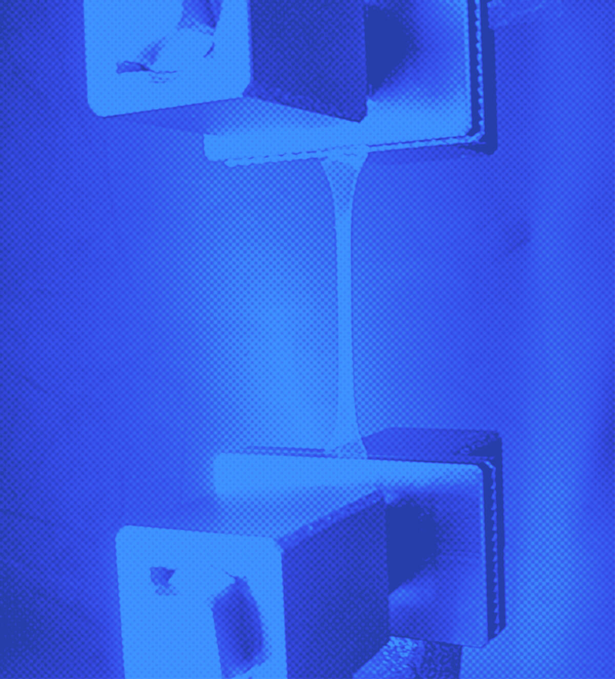
 A conceptual illustration of the reversible, light-induced deformation of a perovskite crystal lattice, a discovery that could enable new classes of responsive semiconductor devices.Davis Today
Researchers at the University of California, Davis have discovered that halide perovskite crystals can reversibly change shape when exposed to light, a phenomenon known as photostriction. This unique property could enable the development of new types of semiconductor devices that respond to light, such as sensors or actuators.
Why it matters
Perovskites are a promising class of semiconductors that offer advantages over traditional materials like silicon and gallium arsenide, including lower manufacturing costs and the ability to tune their properties. The discovery of the photostriction effect in perovskites opens up new possibilities for designing innovative light-responsive devices.
The details
The researchers, led by Professor Marina Leite, shined lasers on perovskite crystals and measured the response of the crystal lattice using X-ray probes. They found that exposure to light causes a dramatic and reversible change in the lattice structure, a phenomenon not seen in other semiconductor materials. By adjusting the composition of the perovskite, the researchers can engineer the specific wavelengths of light that trigger the photostriction effect.
- The research was published on March 3, 2026 in the journal Advanced Materials.
The players
Marina Leite
Professor of materials science engineering at the University of California, Davis and senior author on the research paper.
Mansha Dubey
A graduate student working with Professor Leite on the perovskite research.
Bekir Turedi
A researcher at ETH Zürich who collaborated with the UC Davis team to grow the perovskite crystals used in the study.
Andrii Kanak
A researcher at ETH Zürich who collaborated with the UC Davis team to grow the perovskite crystals used in the study.
Maksym Kovalenko
A professor at ETH Zürich who collaborated with the UC Davis team to grow the perovskite crystals used in the study.
What they’re saying
“They are 'smart materials' that can be tuned to respond to a stimulus in a way we can control. Their chemistry is very different in a way that can be beneficial for creating devices we couldn't build before.”
— Marina Leite, Professor of materials science engineering at UC Davis
“There is a dramatic change in the lattice when you shine light on it, a unique phenomenon that you don't see with silicon or gallium arsenide.”
— Marina Leite, Professor of materials science engineering at UC Davis
“It's not a binary on/off effect; it can be a scaled response, like a dimmer, depending on the light you shine on it.”
— Marina Leite, Professor of materials science engineering at UC Davis
What’s next
The researchers plan to further explore the potential applications of the photostriction effect in perovskites, including the development of new types of light-responsive sensors and actuators.
The takeaway
The discovery of the reversible, tunable photostriction effect in perovskite crystals represents a significant breakthrough that could enable the creation of innovative semiconductor devices with unique light-responsive capabilities, expanding the possibilities for optoelectronics and advanced photonic technologies.